MOSFET Gate Driver IC Overview
MOSFET Gate Driver IC is an ON and Off switching control device for external N-channel MOSFET. Toshiba MOSFET Gate Driver ICs have charge pump and protection circuits and they feature ultra small package (1.2 × 0.8 mm), low quiescent current and wide input voltage. Using them with N-channel MOSFET, this solution acheives small size and low loss power line. Toshiba have a variety lineup of Over Voltage Lock Out function.


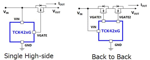
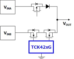
Toshiba MOSFET Gate driver ICs can be used for single high-side, back to back load switches and power multiplexer.
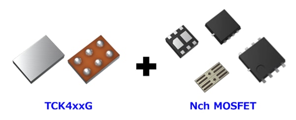
Toshiba Gate Driver ICs can combine many types of Toshiba Nch-MOSFETs. Toshiba have various supports such as providing simulation, switching evaluation and SOA.

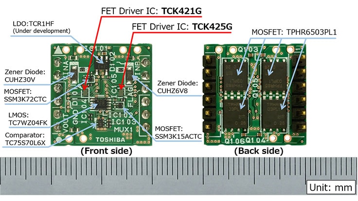
Power multiplexer circuit with 2 input and 1 output is implemented on a small PCB.
Please visit and download below for more detail
Recommended product list
| Product Number | TCK401G | TCK402G | TCK420G | TCK421G | TCK422G | TCK423G | TCK424G | TCK425G |
|---|---|---|---|---|---|---|---|---|
| Data Sheet | PDF(526KB) | PDF(3156KB) | ||||||
| Stock Check |  |
 |
 |
 |
 |
 |
 |
 |
| Maximum Input Voltage VIN max |
40 V | |||||||
| Input Voltage Ranges VIN |
2.7 to 28 V | |||||||
| Gate Drive Voltage VGATE |
4 to 10 V (VIN dependence) | 10 V | 5.6 V | |||||
| Package | WCSP6E (1.2 × 0.8 mm, t:0.55 mm) |
WCSP6G (1.2 × 0.8 mm, t:0.35 mm) |
||||||
| Over Voltage Lockout Threshold |
28 V | 27.73 V | 23.26 V | 14.29 V | 10.83 V | 6.31 V | ||
| Under Voltage Lockout Threshold |
2.7 V | 2 V | ||||||
| Usage | Common Source (Single Hi-side is OK) |
Common Drain (Single Hi-side is OK) |
||||||
Related information
Queries about purchasing, sampling and IC reliability
Stock Check & Purchase
require 3 characters or more.
Through this website you are able to proceed to the website of our distributors ("Third Party Website") which is not under the control of Toshiba Corporation and its subsidiaries and affiliates (collectively "Toshiba"). The Third Party Website is made available to you as a convenience only and you agree to use the Third Party Website at your own risk. The link of the Third Party Website does not necessarily imply a recommendation or an endorsement by Toshiba of the Third Party Website. Please be aware that Toshiba is not responsible for any transaction done through the Third Party Website, and such transactions shall be subject to terms and conditions which may be provided in the Third Party Website.

