High withstand voltage (reverse voltage) characteristics of SiC SBDs
Silicon carbide (SiC) is a wide-bandgap semiconductor with a bandgap of 3.26 eV, much higher than that of silicon (Si) (=1.12 eV). SiC provides high electric breakdown field and high thermal conductivity because of high atomic bond due to a low lattice constant (i.e., a short atom-to-atom distance).
Comparisons of physical properties between Si and SiC
| Characteristics | Unit | Si | 4H-SiC |
|---|---|---|---|
| Bandgap | eV | 1.12 | 3.26 |
| Electron mobility, μe | cm2/Vs | 1400 | 1000/1200 |
| Hole mobility, μh | 600 | 120 | |
| Electric breakdown field, Ec | V/cm | 3.0×10⁵ | 2.8×10⁶ |
| Thermal conductivity, λ | W/cmK | 1.5 | 4.9 |
| Saturation electron drift velocity, Vsat | cm/s |
1.0×10⁷ | 2.2×10⁷ |
| Relative dielectric constant, ε | 11.8 | 9.7/10.2 |

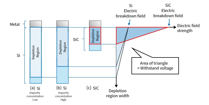
When an SBD with a conventional structure is reverse-biased, the depletion region extends into the semiconductor as shown below. The area of the triangle formed by the electric breakdown field and the depletion region width represents the withstand voltage of an SBD. The depletion region depth is inversely proportional to the dopant concentration. Increasing the dopant concentration helps reduce the resistance of silicon and therefore the forward voltage (VF) of the SBD, but at the expense of withstand voltage (i.e., triangle area). The electric breakdown field of SiC is nearly 10 times that of silicon. As shown below, it is therefore possible to increase the withstand voltage (i.e., triangle area) of a SiC SBD relative to a Si SBD, even if it is heavily doped.
In addition, since the depletion layer is less stretched by the higher concentration, the thickness of the chip can be thinner than in the case of Si. The thickness of the semiconductor (Si or SiC) can be considered as series resistance in the forward direction, and so the forward voltage can be improved by reducing the thickness.
SiC schottky barrier diodes
Related information
Queries about purchasing, sampling and IC reliability
Stock Check & Purchase
require 3 characters or more.
Through this website you are able to proceed to the website of our distributors ("Third Party Website") which is not under the control of Toshiba Corporation and its subsidiaries and affiliates (collectively "Toshiba"). The Third Party Website is made available to you as a convenience only and you agree to use the Third Party Website at your own risk. The link of the Third Party Website does not necessarily imply a recommendation or an endorsement by Toshiba of the Third Party Website. Please be aware that Toshiba is not responsible for any transaction done through the Third Party Website, and such transactions shall be subject to terms and conditions which may be provided in the Third Party Website.

